Silicon Photonics Probe Stations │ Probe Stations Optimized for NIR/NUV

Silicon photonics merges two technologies-integrated circuits and optical communications, which have evolved along parallel but separate paths.

Each offers distinct advantages. Silicon-based IC fabrication now integrates literally billions of transistors onto a single substrate. Laser-based optical communications produce very high bandwidths and low-loss signal transmission over long distances.

When combined via Silicon photonics (SiPh), they offer new possibilities in transmission speed, scalability, energy efficiency and cost reduction.  Over time, Silicon photonics (SiPh), will scale down from data center applications to interconnects on individual chips. Eventually, hundreds of cores on a single IC could be interconnected through an on-chip optical mesh.

Functionality

  • Horizontal die-level edge coupling: lowest coupling loss and highest accuracy in test results
  • Wafer-level edge coupling: innovative technology aligns fibers/arrays in a wafer-level trench Vertical Coupling
  • Industry standard for vertical coupling to wafer-level grating couplers
  • Parented solution available that enables minimized air flow impact at cold temperatures to the fibers/fiber arrays for stable and repeatable measurement results.
  • Chucks up to 450mm with mounting solutions for samples as large as 29”x29

Modular and Upgradeable

  • -65C to 400C thermal testing
  • Manual/Motorized/Semiautomatic upgrades
  • Shielding enclosures, Safety Interlock

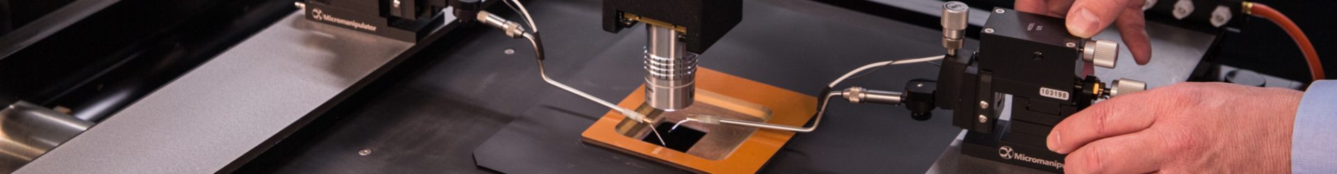
Micron level fiber positioning

Light tight & Atmospheric Environments

Motorized and automated

-65C to 400C Thermal

Request Quote

Website Management Provided by Genacom